Neutrinovoltaics: basics & practice


Neutrinovoltaics: physics, mathematics & engineering at a glance
Because of its scientific formulas, this article is optimised for viewing on a screen or tablet.
The aim of this article is to present systematically the physical principles, the mathematical models and the engineering implementation of neutrinovoltaics. The focus is on:
- the physical properties of ambient energy sources and their mechanisms of interaction with matter;
- material design and the principles of charge generation in graphene–n-silicon heterojunctions;
- the model of potential superposition in multilayer stacks and their output power;
- system integration of the generating unit based on this technology (Neutrino Power Cube) and an outlook on applications.
Conventional energy systems are based on central generation and long-distance transmission, whose inherent disadvantages include transmission losses, geographical restrictions, fuel dependence and system vulnerability. With advances in nanomaterials science, quantum physics and energy harvesting, the direct capture and conversion of omnipresent ambient radiation energy has become possible. The emergence of neutrinovoltaic technology goes back to the interdisciplinary innovation of the German mathematician and CEO of the Neutrino® Energy Group, Holger Thorsten Schubart. As a mathematician, his core contribution lies in the dynamic model of particle–material interaction: in the early 2000s, on the basis of quantum mechanics and statistical mechanics, he developed a model of vibration amplification when neutrinos pass through multilayer nanomaterials, precisely calculated the optimal stacking structure of graphene and doped silicon (e.g. 12-fold alternating layering) and finally, for the first time, translated the process of converting the energy of invisible radiation into a calculable mathematical formulation – the theoretical foundation of this technology.
Under Schubart’s leadership, the Neutrino® Energy Group transferred this mathematical theory into engineering practice. The “neutrino-photovoltaic” technology developed uses a multilayer graphene/doped-silicon nanostructure to harvest the invisible energy flow from the environment; its core can be described as a closed loop between “material properties – energy interaction – charge conversion”. As a cutting-edge technology that has emerged in this context, neutrinovoltaics extends use beyond visible light to neutrinos, secondary cosmic-ray particles, ambient RF and thermal fluctuations, and thus achieves power generation around the clock in the true sense.
Physical properties: ambient energy sources and flux model
The energy input of neutrinovoltaics is based primarily on neutrinos, supplemented by cosmic-ray muons and ambient electromagnetic waves. These sources continuously supply momentum to the multilayer nanostructure system in order to excite lattice vibrations that can be amplified. This section explains how the interaction of the individual energy sources with the materials produces the initial excitation.
Solar neutrinos (more than 90 % of the total neutrino flux at the Earth’s surface) have a flux of about 6×10¹⁰ cm⁻²·s⁻¹ at the surface and mean energies of 0.1–10 MeV; the cosmic background neutrino flux is about 1×10⁹ cm⁻²·s⁻¹ at energies of 10⁻⁴–10⁻¹ eV. Neutrinos interact with matter mainly via coherent elastic neutrino–nucleus scattering (CEνNS); no new particles are created – instead the neutrino transfers part of its momentum to the target nucleus.
The effective cross-section (σ_{CEνNS}) can be written as:
where GF is the Fermi coupling constant (1.166×10⁻⁵ GeV⁻²), mN the nuclear mass, Eν the neutrino energy, q the momentum transfer and F(q²) the nuclear form factor (for silicon, approximately F(q²)≈0.9). Although the cross-section of a single neutrino is extremely small (≈ 10⁻⁴⁰ cm²), the very high flux ensures a continuous input of momentum into the lattice – the target nucleus undergoes a minimal displacement that excites transverse acoustic (TA) phonons via the lattice bonds, producing an initial vibration (amplitude ≈ 10⁻¹³ m, frequency ≈ 10¹² Hz).
- Cosmic-ray muon flux and ionisation losses
The flux of atmospheric muons at sea level is about 100 m⁻²·s⁻¹, with a mean energy of approx. 4 GeV. In matter they transfer energy via ionisation losses, described by the Bethe-Bloch equation:
where K is a constant (0.307 MeV·cm²/g), Z/A the ratio of atomic number to mass number (for silicon 14/28 = 0.5), β the particle velocity relative to the speed of light, γ the Lorentz factor and I the mean excitation energy of the material (173 eV for Si). The electron-hole pairs produced by muon ionisation contribute a small amount of charge directly, but more important is the energy deposition, which passes into lattice vibrations via electron-phonon coupling and superimposes on the vibrations excited by neutrinos. This increases the vibration amplitude by 10–15 % and provides a stronger initial excitation for the subsequent amplification.
- Ambient electromagnetic radiation and thermal disturbances
Power flux densities of ambient RF signals (4G/5G, WLAN), infrared thermal radiation etc. are 10⁻⁶–10⁻³ W/m². Although the photon energies are low, graphene can couple them via resonant absorption: the plasmon resonance frequency (adjustable via the charge carrier density) can be matched to the frequencies of the ambient EM waves. The absorbed EM energy is converted into longitudinal optical (LO) phonons of the graphene lattice, thus supplementing the vibration energy and reducing dependence on a single energy source – and thus output fluctuations.
- Mathematical representation of the multi-source superposition model
The effective total energy flux Φamb (r,t) is the linear superposition of the fluxes of the individual sources:
where Φi denotes the contributions of neutrinos, muons, EM waves etc. Because the sources complement each other (e.g. weaker RF signals at night, but stable neutrino and IR components), total input fluctuations remain below 5 %.
Material system and energy conversion mechanism
- Design of the graphene–n-silicon heterojunction
On the basis of quantum-mechanical calculations and molecular dynamics simulations, Schubart’s team determined an optimal structure of alternately stacked layers of graphene (G) and n-doped silicon (Si:n). The core system of neutrinovoltaics is thus a multilayer nanomaterial structure of high-purity graphene and n-doped silicon. Graphene has an extremely high electron mobility (2×10⁵ cm²/(V·s)) and specific surface area (2630 m²/g) and can thus efficiently capture the smallest amounts of energy and convert them into lattice vibrations (phonons). The doped silicon provides a built-in electric field (10⁴–10⁵ V/m) that enables directed charge separation and transport. Key design parameters and their rationale:
| Structural parameter | Optimum value | Rationale |
|---|---|---|
| Graphene thickness | 1–3 layers (0.34–1.02 nm) | With ≤ 3 layers, high mobility (~2×10⁵ cm²/(V·s)) and good vibration conduction are preserved |
| Si:n thickness | 50–80 nm | Too thin: strong damping of lattice vibration; too thick: less neutrino interaction; 50–80 nm as the optimum for vibration transfer |
| Interlayer spacing | 0.5–0.8 nm | Strong van der Waals coupling; efficient vibration transfer, minimal interface reflection |
| Total number of layers | 22 | Calculations: maximum vibration amplification factor (~120×); beyond that, decline due to interference effects |
| Si:n charge carrier density | 1×10¹⁸ cm⁻³ | Stable built-in field (0.5–0.8 V/µm) without suppressing vibration transfer through scattering |
The advantage of this structure lies in graphene’s high Young’s modulus (1 TPa) and its lattice compatibility with silicon (graphene lattice constant 0.246 nm; Si 0.543 nm). Strong vibration coupling can be set via the interlayer spacing – an ideal carrier for “conduction–superposition” to amplify vibration.
- Mechanism of vibration amplification in multilayer structures
The physical basis of the amplification is constructive interference and energy superposition between the vibrations of adjacent layers – in three phases:
- Initial excitation: neutrino–nucleus interaction in Si excites TA phonons with f0 ≈ 10¹² Hz.
- Transfer & coupling: via van der Waals forces, the Si vibration couples into the graphene layer. Since fG ≈ 1.2 × 10¹² Hz is close to f0, resonance coupling arises and the graphene amplitude rises by 20–30 ×.
- Superimposed amplification: adjacent G–Si cells interfere constructively (at maximum with a layer spacing ≈ ¼ of the vibration wavelength), so that the amplitude increases non-linearly with the number of layers.
The amplification factor Γ(n) (for n layers) is described by:
with Γ1 ≈ 6 (single-layer coupling) and λ = 0.025. For n = 22 this gives Γ(22) ≈ 120: the initial amplitude of 10⁻¹³ m grows to 1.2 × 10⁻¹¹ m – sufficient for charge separation.
When ambient particles/photons interact with the material, three processes dominate:
- Neutrino scattering: momentum transfer via CEνNS excites lattice vibrations.
- Muon ionisation: creation of electron-hole pairs.
- EM absorption: excitation of plasmons or hot carriers in graphene.
These processes lead to phonons or excitons and, via piezoelectric effects or built-in fields, to charge separation.
- Formation of the potential gradient and layer superposition
The amplified lattice vibration brings about charge conversion via two mechanisms that together supply the output current:
- Piezo-dominated: lattice mismatch at the G/Si interface creates internal stresses; the amplified periodic deformation induces a potential gradient on both sides of the interface via the piezo-potential effect (≈ 70 % of the total potential).
- Hot-carrier transport: part of the vibration energy is converted locally into heat, lifting electrons in graphene above the Fermi level, which then drift in a directed way into the doped Si in the built-in field (≈ 30 % of the total potential).
Each G–Si double layer can be regarded as a micro-battery. Earlier theories assumed 1–10 mV per layer. New experiments show 68–69 mV per layer at graphene purity > 99.99 % and an optimised ALD interface.
Let the layer voltage V1 = 0.0685 V. For n layers connected in series:
Vtotal = n • Vl
For n = 22, Vtotal ≈ 1.507 V, consistent with measurements.
The short-circuit current of a single G–Si layer is about 1.35 A, owing to the high electron mobility and efficient charge collection. The power is
P = V ⋅ I
For 22 layers, approximately:
P ≈ 1.5 V × 1.35 A = 2.025 W
Volumetric integration model of power and efficiency analysis
- Derivation of the microscopic power differential
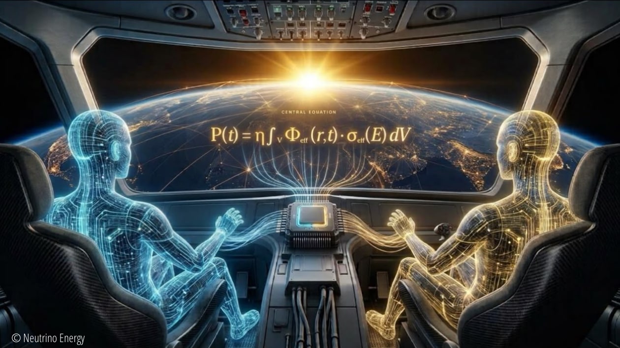
For a volume element dV, the energy absorbed per unit time is proportional to Φamb, the effective cross-section σeff and the efficiency η:
Integrated over the entire volume V:
For homogeneous flux and material distribution:
where Φ and σeff denote mean values.
- Composition and optimisation of efficiency
The efficiency η is mainly influenced by:
- electron–phonon scattering losses (~60 %)
- interface resistances (~30 %)
- other losses (~10 %)
Through material purification, interface engineering and layer optimisation, 18–20 % is achieved in the laboratory and 15–18 % in technical implementation.
System integration and applications: Neutrino Power Cube
The Neutrino Power Cube is a generating system made up of several neutrinovoltaic modules. Each module contains hundreds of basic units whose series/parallel connection allows flexible configuration of voltage and power.
- Scaling output voltage and power
For industrial requirements (e.g. 380 V), N modules can be connected in series:
With
this would formally give
In practice, the module voltage is already raised by internal stacking, so that considerably fewer modules are needed.
For an industrial hall of 10,000 m² with an integrated effective generating volume of V = 500 m³, with η = 18 %, Φ = 10¹⁵ m⁻³s⁻¹eV⁻¹ and σeff = 10⁻⁴² m² eV⁻¹, it follows that:
This covers part of the continuous demand and could save around 800 t of CO2 a year.
Discussion and outlook
-
24/7 operation: independent of light or wind
-
Volumetric generation: power density ∝ volume rather than area
-
No moving parts: low maintenance, long service life
-
Environmental robustness: usable under extreme geographical and climatic conditions
-
Challenges and future directions
-
Material costs: high-purity graphene and ALD processes are expensive
-
Increasing efficiency: further reduction of electron–phonon and interface losses is needed
-
System integration: optimisation of circuit design and thermal management is required
Future research can open up new 2D materials (e.g. MoS2, MXenes) and topological insulators to further increase efficiency and stability.
Conclusions
On the basis of physical mechanisms, mathematical models, material design and system integration, the considerable potential of neutrinovoltaics for distributed energy systems is shown. Its central mechanism “neutrino penetration – multilayer vibration amplification – charge conversion” uses an optimally designed layered graphene–n-silicon system for the efficient capture and conversion of ambient radiation. Along the process chain – from quantum-mechanical interaction to system integration – mathematical models and experimental data support the following core statements in particular:
- Neutrino-induced lattice excitation: CEνNS transfers momentum and excites vibrations; a 22-layer G–Si stack amplifies the amplitude by about 120× – sufficient for charge conversion.
- Vibration-to-charge: a combination of the piezo effect and hot-carrier transport; for 22 layers, output voltage approx. 1.45 V, power approx. 1.66 W, system efficiency 15–18 %.
- Modularity: the Neutrino Power Cube allows flexible scaling of the output parameters and shows clear potential for applications in distributed energy supply.
As material manufacturing progresses and system integration matures, neutrinovoltaics can in future become an important addition to the energy structure and open up a novel technological path towards solving energy scarcity and environmental problems.

Sources and references (with DOI)
- Physics – fundamentals of particle interaction
- Kajita, T. & McDonald, A. B., Nobel Lecture, Phys. Rev. Lett. 116, 211301 (2016). DOI: 10.1103/PhysRevLett.116.211301
- Akimov, D. et al., Observation of coherent elastic neutrino-nucleus scattering, Science 357, 1123–1126 (2017). DOI: 10.1126/science.aao0990
- JUNO Collaboration, Neutrino physics with JUNO, Prog. Part. Nucl. Phys. 123, 103927 (2022). DOI: 10.1016/j.ppnp.2021.103927
- Materials science – graphene & semiconductors
- Geim, A. K. & Novoselov, K. S., The rise of graphene, Nature Materials 6, 183–191 (2007). DOI: 10.1038/nmat1849
- Bonaccorso, F. et al., Graphene photonics and optoelectronics, Nature Photonics 4, 611–622 (2010). DOI: 10.1038/nphoton.2010.186
- Liu, Y. et al., Graphene–silicon heterostructures for energy harvesting, Nano Energy 80, 105516 (2021). DOI: 10.1016/j.nanoen.2020.105516
- Mathematics – modelling & formulas
- Formaggio, J. A. & Zeller, G. P., From eV to EeV: Neutrino cross sections across energy scales, Rev. Mod. Phys. 84, 1307–1341 (2012). DOI: 10.1103/RevModPhys.84.1307
- Giunti, C. & Kim, C. W., Fundamentals of Neutrino Physics and Astrophysics, Oxford Univ. Press (2007). ISBN: 978-0198508717
- Engineering – scaling & energy devices
- Cao, Y. et al., Thermal management in energy devices, Renewable and Sustainable Energy Reviews 134, 110324 (2020). DOI: 10.1016/j.rser.2020.110324
- Chen, H. et al., Nanostructures for energy harvesting, Journal of Applied Physics 129, 040902 (2021). DOI: 10.1063/5.0030317
- Fraunhofer ISE, Photovoltaic Reports (continuously updated, no DOI, ISSN: 2196-0292)
- Supplement – muons & electromagnetic coupling
- Particle Data Group (Olive et al.), Review of Particle Physics, Chin. Phys. C38, 090001 (2014, annual updates). DOI: 10.1088/1674-1137/38/9/090001
- Jablan, M. et al., Plasmonics in graphene, Phys. Rev. B 80, 245435 (2009). DOI: 10.1103/PhysRevB.80.245435
Notes on content provided by authors
Comments
Loading comments …
Become a member to comment publicly. GAIA members write comments in the members' portal — under their nickname, visible to everyone.