Neutrinovoltaics: when materials become energy converters


A new paradigm of energy generation
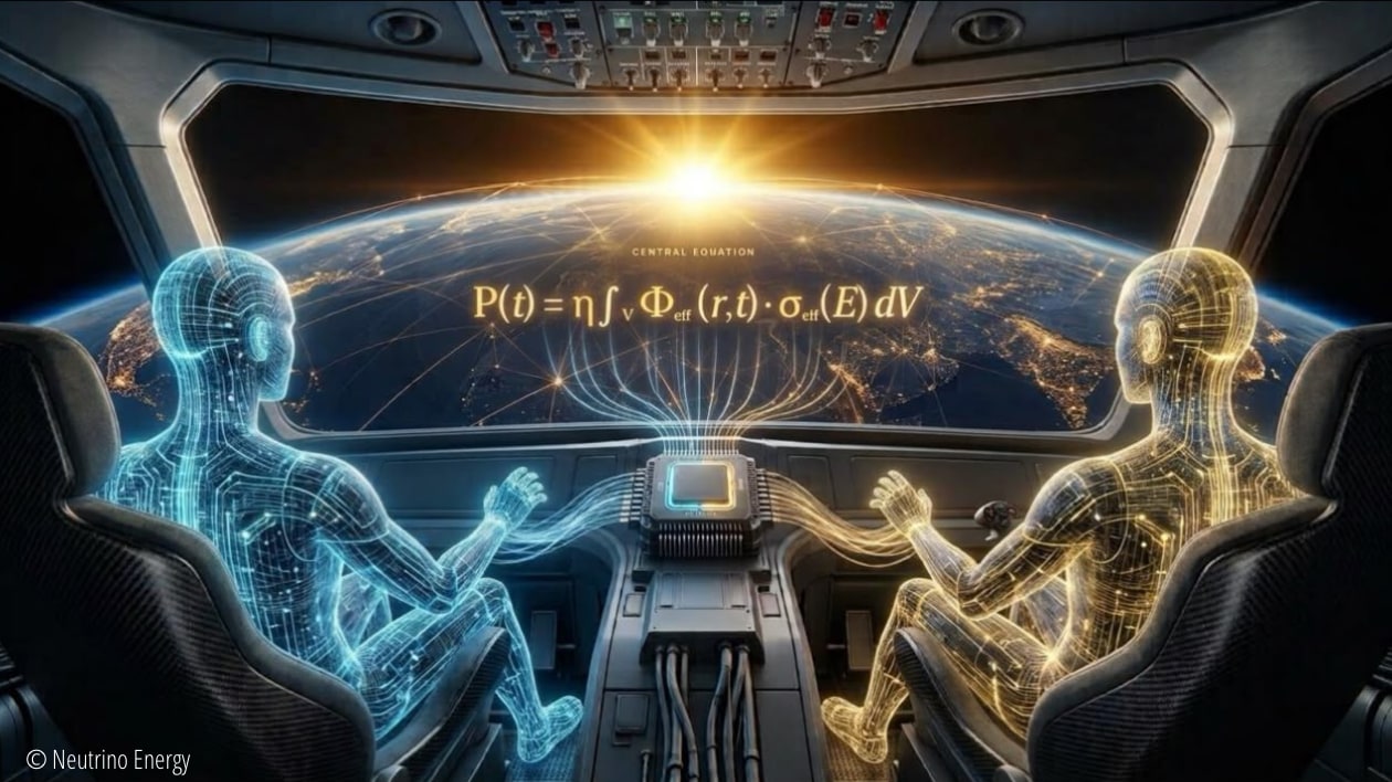
For a long time, matter was regarded as a passive component of technical structures in the energy system. Steel bears loads, concrete stabilises buildings and silicon serves as a semiconductor in electronic components. Energy itself is traditionally obtained from external sources – for example through chemical combustion, sunlight or mechanical turbines. Neutrinovoltaics describes a different approach. Here, materials are structured in such a way that they directly couple permanently present energy flows from the environment and convert them into electrical energy. The mathematical foundation of this technology describes the electrical power of such a system by
The equation states that the power generated is proportional to the ambient flux and to the effective interaction of the material structure.
Ambient energy as a continuous resource
The physical space around the Earth is by no means energetically empty. Rather, there are permanent background flows, including:
- electromagnetic fields
- thermal fluctuations
- micromechanical vibrations
- cosmic particles
- solar neutrinos

Solar neutrinos alone pass through the Earth with a flux density of more than
These flows form the energy source for neutrinovoltaic materials.
Nanostructured materials
The technical implementation is based on a nanoscale heterostructure. The system consists of:

- high-purity copper foil as substrate
- currently 9 alternating layers of graphene and n-doped silicon
- functional interface layers in the sub-nanometre range
Owing to its high electron mobility and surface area, graphene acts as an efficient energy absorber. The doped silicon creates an internal electric field of
This field enables the directed separation of charge carriers. Experiments show that a stacked structure of about nine active layers represents an optimal balance between energy accumulation and interference.
From nanoprocess to current flow


The energy conversion process takes place in several physical stages.
First, ambient particles or electromagnetic fields transfer momentum to atomic nuclei in the material. This creates lattice vibrations, so-called phonons. These vibrations couple with electrons and generate electron-hole pairs.
The internal electric field separates these charges and creates directed currents. Through billions of parallel nanostructures, these currents add up to a macroscopically measurable current.
The output power always remains within the bounds of energy conservation
Role in the future energy system
Neutrinovoltaic technologies are not intended as a replacement for classical energy sources. Rather, their potential lies in providing continuous background energy. Possible applications are:
- decentralised power supply
- energy supply for remote regions
- autonomous sensors
- space travel and extreme environments
- complementing fluctuating renewable energies
Since the energy source is independent of weather, time of day or fuels, such systems can take on a stabilising role in hybrid energy structures.
Technical implementation (industrial)

The technical implementation of the neutrinovoltaic structure is based on a multilayer nanoscale heterostructure system.
The substrate made of high-purity copper foil plays a central role. This copper foil usually has a purity of over 99 per cent and a thickness of about 8 to 22 micrometres. Owing to its high electrical conductivity and good mechanical properties, it serves both as a stable mechanical carrier for the nanostructures above it and as an efficient collection path for the electrical charges generated. In this way, the microscopic charge currents generated in the active material can be reliably brought together and carried off as a macroscopic electric current.
The active layers of the material structure described consist of alternating stacks of graphene and n-doped silicon.
Graphene is characterised by an exceptionally high electron mobility of about 2 × 10⁵ cm²/(V⋅s) and a very large specific surface area of around 2630 m²/g.
These properties enable a particularly efficient interaction with coupled-in energy flows at the nanoscale. The n-doped silicon fulfils a complementary function within the structure: it generates an internal electric field in the range of 10⁴–10⁵ V/m. This field ensures the directed separation of the electron-hole pairs created in the material and thus enables the conversion of the excited states into a usable electric current.
Between the graphene and silicon layers is a functional interface layer about 0.5 to 0.8 nanometres thick.
This extremely thin layer enables strong coupling of the two materials via van der Waals forces and ensures that energy in the form of lattice vibrations can be transferred efficiently between the layers. Experimental studies show that the performance of the structure depends strongly on the number of active layers. A stack of nine active layers has proved optimal. With fewer layers, energy cannot accumulate sufficiently in the material, while too many layers lead to interference effects that dampen the vibrations and thus reduce energy conversion.
The energy conversion mechanism is based on a sequence of several physical processes taking place in the nanoscale material system.
- First, momentum transfer takes place, in which neutrinos and other ambient flows transfer energy to atomic nuclei within the active material layers.
- This excitation then produces lattice vibrations in the crystal lattice, so-called phonons. In a further step, these lattice vibrations couple with the electrons of the material, creating electron-hole pairs.
- The internal electric field present in the n-doped silicon then provides directed charge separation, in which electrons and holes move in opposite directions.
- The microscopic currents produced in this way are added across layers via billions of nanostructures working in parallel and reinforce each other.
- Finally, the electrical impedance is matched so that the current generated can be delivered stably to an external load and extracted as usable electrical energy.
Efficiencies of over 30 % are stated under laboratory conditions. Energy generation is continuous, as the ambient flows are permanently present.
Conclusion: Energy and independence
Neutrinovoltaics is a prime example of a new perspective in materials science. Materials are no longer regarded exclusively as structural components, but as active elements of the energy infrastructure.
In the long term, this perspective opens up the possibility of a more decentralised energy supply. If materials themselves can take over energy conversion, new degrees of freedom arise for technical systems – from autonomous devices to independent energy units in buildings and infrastructure.
Technological innovation in material structure could thus not only improve the efficiency of energy conversion but also contribute to greater energy independence and resilience of modern societies.
Notes on content provided by authors
Comments
Loading comments …
Become a member to comment publicly. GAIA members write comments in the members' portal — under their nickname, visible to everyone.